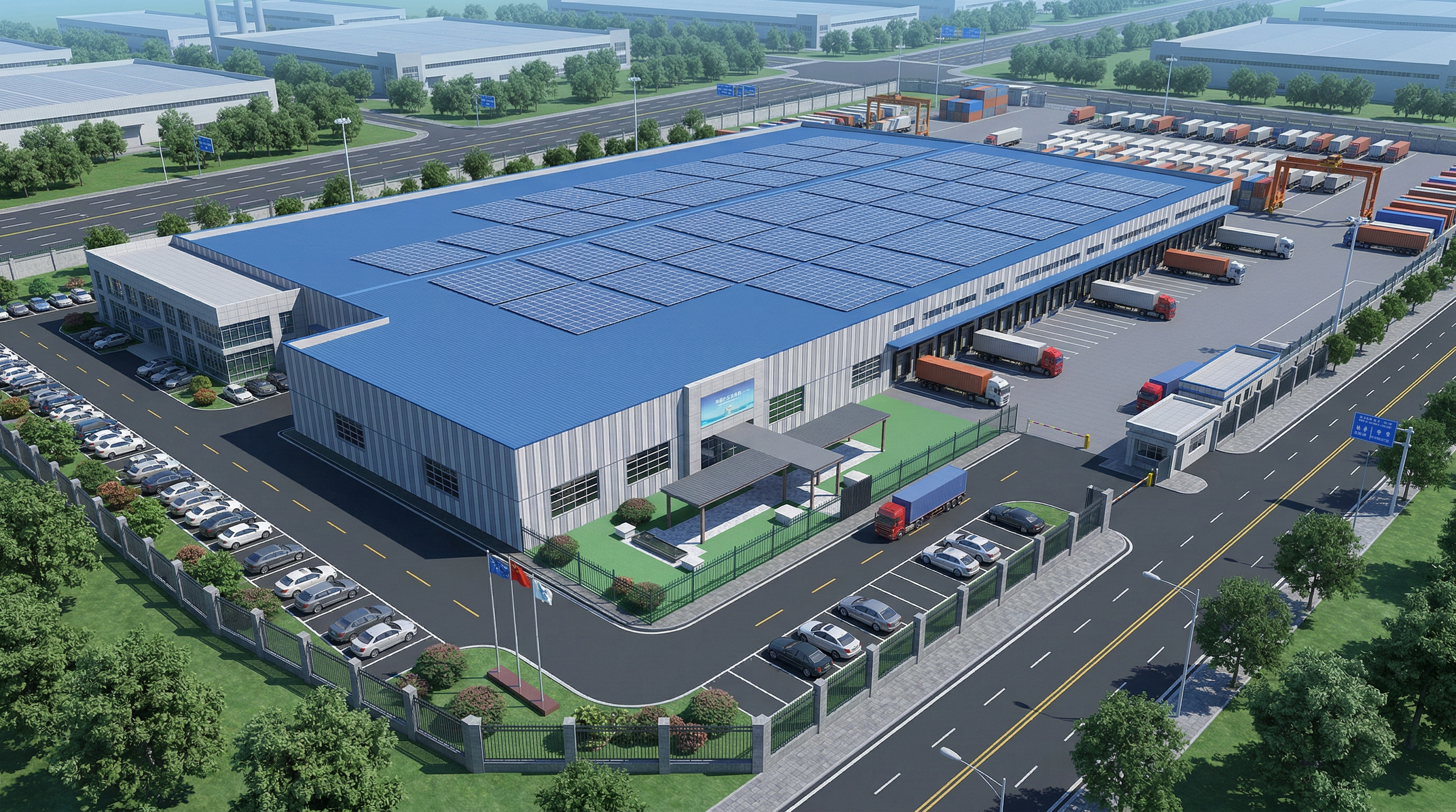
Built for volume TLFN production. A 30,000+ sqft US factory with over 1,000 tools across multiple cleanroom bays, producing thousands of wafers per month under US-controlled operations.
NantOptiFab’s 30,000+ sqft US fab consolidates every step of TLFN fabrication—from in-house LNOI wafer creation (ion slicing and bonding from raw crystal) through to packaged die—under one roof. 3,000+ sqft of Class 100 (ISO 5) photolithography cleanroom, 7,000+ sqft of Class 1k (ISO 6) production area, fiber pigtailing and packaging lines, and space qualification test infrastructure. No outsourcing, no offshore dependencies.
Our 1,000+ tools span every process step needed to fabricate TLFN photonic circuits at volume.
Deep-UV and e-beam lithography systems for sub-100 nm waveguide patterning. Stepper and contact aligners for high-throughput production runs across 6-inch LNOI wafers.
Argon ion milling and RIE systems optimized for lithium niobate. Chemical-mechanical planarization for surface smoothing post-etch, achieving sub-nanometer RMS roughness.
PECVD, sputtering, and e-beam evaporation for SiO2 cladding, metal electrodes (Au, Ti, Cr), and dielectric layers. Thickness control to ±1% across full wafers.
High-voltage poling stations with patterned electrodes for domain inversion. Automated poling with real-time current monitoring for uniform quasi-phase-matched gratings.
Automated probe stations for optical insertion loss, modulator Vπ and bandwidth, and waveguide propagation loss mapping. 100% wafer-level screening before dicing.
Precision dicing, fiber pigtailing with active alignment (<1 dB coupling loss), wire bonding, hermetic sealing, and final module assembly. Space qualification testing to MIL-STD-1540 for LEO and GEO deployment.
Today, virtually all TLFN wafer fabrication occurs overseas. NantOptiFab is building the domestic capacity the US needs—eliminating single-source risk for the telecom, defense, and quantum industries. ITAR-compliant, on US soil.
TLFN is critical to next-generation defense photonics—EW sensors, secure quantum comms, and radiation-hard optical links. Our US-controlled fab provides a trusted, classified-capable supply chain for DoD and IC customers.
Schedule a visit to our US facility. Meet our process engineers, tour the cleanroom, and discuss how we can support your TLFN production needs.